- 您现在的位置:买卖IC网 > Sheet目录1233 > NCP1652L48VGEVB (ON Semiconductor)BOARD EVAL 100W 48V NCP1652 PFC
�� �
�
�NCP1652,� NCP1652A�
�the� 2� ?� stage� solution.� As� a� result,� potentially� higher�
�leakage� inductance� induces� higher� voltage� spikes� (like�
�the� one� shown� in� Figure� 53)� on� the� MOSFET� drain.�
�V� in�
�Active�
�Clamp�
�V� out�
�This� may� require� a� MOSFET� with� a� higher� voltage�
�rating� compared� to� similar� dc� ?� input� flyback�
�applications.�
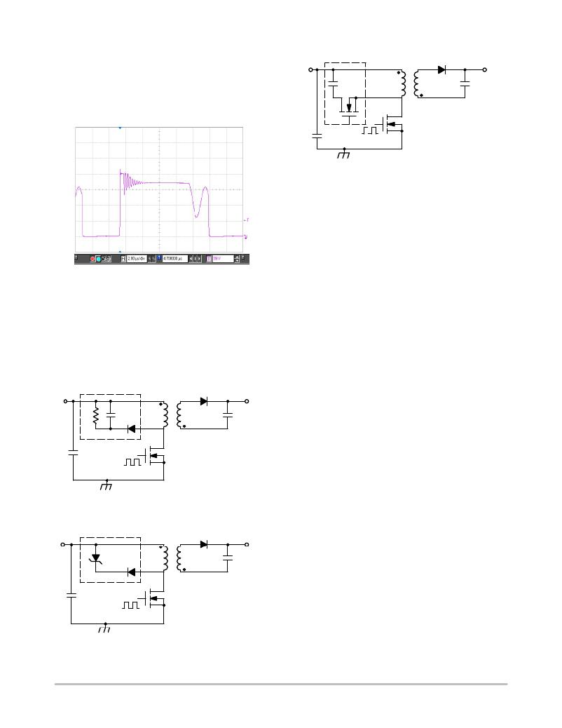
�Figure� 56.� Active� Clamp�
�The� first� two� methods� result� in� dissipation� of� the� leakage�
�energy� in� the� clamping� circuits� –� the� dissipation� is�
�proportional� to� LI� 2� where� L� is� the� leakage� inductance� of� the�
�transformer� and� I� is� the� peak� of� the� switch� current� at�
�turn� ?� off.� An� RDC� snubber� is� simple� and� has� the� lowest� cost,�
�but� constantly� dissipates� power.� A� TVS� provides� good�
�voltage� clamping� at� a� slightly� higher� cost� and� dissipates�
�power� only� when� the� drain� voltage� exceeds� the� voltage�
�Figure� 53.� Typical� Drain� Voltage� Waveform� of� a�
�Flyback� Main� Switch�
�There� are� a� few� methods� to� clamp� the� voltage� spike� on� the�
�main� switch,� a� resistor� ?� capacitor� ?� diode� (RCD)� clamp,� a�
�transient� voltage� suppressor� (TVS)� or� an� active� clamp� using�
�a� MOSFET� and� capacitor� can� be� used� as� shown� in�
�Figures� 54� to� 56.�
�rating� of� the� TVS.�
�The� active� clamp� circuit� provides� an� intriguing� alternative�
�to� the� other� methods.� It� requires� addition� of� a� MOSFET� and�
�a� high� voltage� capacitor� as� part� of� the� active� clamp� circuit,�
�thus� adding� complexity,� but� it� results� in� a� complete� reuse� of�
�the� leakage� inductance� energy.� As� a� result,� the� transformer�
�construction� is� no� longer� critical� and� one� can� use� cheaper�
�cost� solution.� Also,� the� active� clamp� circuit� reduces� the�
�voltage� stress� on� the� primary� switch� and� that� can� lead� to�
�V� in�
�R�
�C�
�D�
�RCD�
�Clamp�
�V� out�
�usage� of� lower� cost� or� lower� on� resistance� (R� DS(on)� )�
�MOSFET.� Finally,� the� turn� ?� on� switching� losses� are�
�eliminated� because� the� active� clamp� circuit� allows� the�
�discharge� of� the� MOSFET� C� OSS� capacitance� prior� to� the�
�turn� ?� on.� The� energy� stored� in� the� leakage� inductance� is�
�utilized� for� this� transition.�
�In� many� applications,� the� added� complexity� of� the� active�
�clamp� circuit� may� not� be� justified.� However,� the� OUTB� of�
�the� NCP1652� is� also� usable� for� another� purpose,�
�synchronous� rectification� control.� Synchronous�
�Figure� 54.� RCD� Clamp�
�rectification� for� flyback� converters� is� an� emerging�
�requirement� for� flyback� converters.� The� OUTB� signal� from�
�NCP1652� is� ideal� for� interfacing� with� a� secondary� side�
�V� in�
�TVS�
�TVS�
�Clamp�
�V� out�
�synchronous� rectifier� controller� such� as� NCP4303� as� shown�
�in� Figure� 57.� As� shown� in� Figure� 57,� using� the� OUTB�
�(coupled� through� pulse� transformer� or� Y� ?� capacitor)� as� a�
�trigger� for� the� NCP4303� allows� guaranteed� turn� ?� off� of� the�
�secondary� side� synchronous� MOSFET� prior� to� turn� ?� on� of�
�the� primary� switch.� In� any� CCM� flyback� converter,� this� is� a�
�critical� requirement� to� prevent� cross� ?� conduction� and�
�NCP1652� and� NCP4303� combination� is� the� first� such�
�chipset� that� guarantees� the� operation� without�
�cross� ?� conduction.�
�Figure� 55.� TVS� Clamp�
�http://onsemi.com�
�20�
�发布紧急采购,3分钟左右您将得到回复。
相关PDF资料
NCP1653EVB
BOARD EVAL FOR NCP1653
NCP2993FCT2GEVB
BOARD EVAL NCP2993 AUDIO PWR AMP
NCP345SNT1G
IC DETECTOR OVER VOLTAGE 5TSOP
NCP346SN2T1G
IC DETECTOR OVER VOLTAGE 5TSOP
NCP347MTAITBG
IC OVERVOLTAGE PROT CTRLR 10WDFN
NCP348AEMUTBG
IC MOSFET DRIVER DUAL 12V 10LLGA
NCP360MUTXG
IC CTLR USB POS OVP FET 6-UDFN
NCP361MUTBG
IC USB OVERVOLT PROT CTRLR 6UDFN
相关代理商/技术参数
NCP1653ADR2
功能描述:功率因数校正 IC Fixed Frequency RoHS:否 制造商:Fairchild Semiconductor 开关频率:300 KHz 最大功率耗散: 最大工作温度:+ 125 C 安装风格:SMD/SMT 封装 / 箱体:SOIC-8 封装:Reel
NCP1653ADR2G
功能描述:功率因数校正 IC Fixed Frequency Current Mode PFC RoHS:否 制造商:Fairchild Semiconductor 开关频率:300 KHz 最大功率耗散: 最大工作温度:+ 125 C 安装风格:SMD/SMT 封装 / 箱体:SOIC-8 封装:Reel
NCP1653ADR2G-CUT TAPE
制造商:ON 功能描述:NCP1653 Series 15 V 6 mA Current-Mode Power Factor Correction Controller SOIC-8
NCP1653AP
功能描述:功率因数校正 IC Fixed Frequency RoHS:否 制造商:Fairchild Semiconductor 开关频率:300 KHz 最大功率耗散: 最大工作温度:+ 125 C 安装风格:SMD/SMT 封装 / 箱体:SOIC-8 封装:Reel
NCP1653APG
功能描述:功率因数校正 IC Fixed Frequency Current Mode PFC RoHS:否 制造商:Fairchild Semiconductor 开关频率:300 KHz 最大功率耗散: 最大工作温度:+ 125 C 安装风格:SMD/SMT 封装 / 箱体:SOIC-8 封装:Reel
NCP1653DR2
功能描述:功率因数校正 IC Fixed Frequency RoHS:否 制造商:Fairchild Semiconductor 开关频率:300 KHz 最大功率耗散: 最大工作温度:+ 125 C 安装风格:SMD/SMT 封装 / 箱体:SOIC-8 封装:Reel
NCP1653DR2G
功能描述:功率因数校正 IC Fixed Frequency Current Mode PFC RoHS:否 制造商:Fairchild Semiconductor 开关频率:300 KHz 最大功率耗散: 最大工作温度:+ 125 C 安装风格:SMD/SMT 封装 / 箱体:SOIC-8 封装:Reel
NCP1653EVB
功能描述:BOARD EVAL FOR NCP1653 RoHS:是 类别:编程器,开发系统 >> 评估演示板和套件 系列:- 标准包装:1 系列:PCI Express® (PCIe) 主要目的:接口,收发器,PCI Express 嵌入式:- 已用 IC / 零件:DS80PCI800 主要属性:- 次要属性:- 已供物品:板